Everything You Ever Wanted to Know About Semiconductors
You’ve undoubtedly heard of semiconductors. They really are everywhere. But while most people have heard of semiconductors, very few people know much about them.
We intend on changing that.
Consider this your introduction to the world of semiconductors. By the end of this article, you’ll be able to discuss the subject confidently, which may not win you many dates but will certainly earn you the respect of electrical engineers.
What is A Semiconductor?
A semiconductor is a physical substance designed to manage and control the flow of current in electronic devices and equipment. It either doesn’t allow a freely flowing electric current or repels the current completely.
A semiconductor sits between a conductor and an insulator and is commonly used in the development of electronic chips, computing components, and devices. It’s generally created using silicon, germanium, or other pure elements.
Semiconductors are created by adding impurities to the element. The conductance or inductance of the element depends on the type and intensity of the added impurities.
There are two basic types of semiconductors. An N-type semiconductor is used when its conductance is higher, or there is a large number of free electrons. A P-type semiconductor is used when its inductance is higher, and there are less free electrons.
Conventional devices and components built by using a semiconductor include, computer memory, integrated circuits, diodes, and transistors.
If you want an in-depth look at how semiconductors are made, here’s a helpful video:
Types of Semiconductor Products
Semiconductor devices are electronic components that utilize the properties of semiconductors to control the flow of electric current. They play a crucial role in modern electronics and are used in a wide range of applications. Here are some of the major types of semiconductor devices:
- Diodes:
- Light Emitting Diodes (LEDs): These diodes emit light when current flows through them, and they are commonly used in displays, indicators, and lighting applications.
- Photodiodes: These diodes generate a current proportional to the amount of incident light, making them useful in light detection and optical communication systems.
- Laser Diodes: Laser diodes produce coherent and monochromatic light and are utilized in various applications, including optical storage, telecommunications, and laser pointers.
- PIN Diodes: These diodes have an intrinsic layer between the P and N layers, making them suitable for applications such as RF switches, photodetectors, and attenuators.
- P-N Junction Diodes: The most basic type of diode, consisting of a P-N junction, which allows current to flow in one direction while blocking it in the reverse direction.
- Schottky Diodes: These diodes have a metal-semiconductor junction, enabling them to switch rapidly and exhibit low forward voltage drop.
- Tunnel Diodes: Tunnel diodes utilize quantum tunneling and have a negative resistance region in their current-voltage characteristics, making them useful in high-frequency oscillators and amplifiers.
- Varactor Diodes: Also known as voltage-controlled capacitors, these diodes change their capacitance based on the applied voltage, commonly used in tuning circuits and voltage-controlled oscillators.
- Avalanche Diodes: These diodes operate in avalanche breakdown mode and are employed in applications such as voltage clamping and noise generation.
- Gunn Diodes: Gunn diodes exhibit a unique negative differential resistance property, used primarily in microwave applications, including oscillators and amplifiers.
- Rectifiers: Diodes used for converting alternating current (AC) to direct current (DC) by allowing current flow in only one direction.
- Zener Diodes: Zener diodes are designed to operate in the reverse breakdown region, maintaining a nearly constant voltage despite changes in current.
- Constant Current Diodes: These diodes provide a constant current regardless of changes in voltage, commonly used in current-limiting applications.
- Backward Diode: A type of diode that exhibits negative resistance, commonly used in microwave applications.
- Gold Doped Diodes: Diodes with gold doping to enhance their performance in high-temperature applications.
- Step Recovery Diodes: These diodes generate extremely fast switching transitions and are utilized in applications such as pulse generation and frequency multiplication.
- Schockley Diodes: A four-layer, three-terminal diode used in triggering and switching applications.
- Transient-Voltage-Suppression (TVS) Diodes: TVS diodes protect electronic circuits from voltage spikes and transients.
- Crystal Detectors: Simple diodes used for detecting radio frequency signals.
- Vacuum Diode: The earliest type of diode that uses a vacuum to control electron flow, mainly found in historical electronics.
- Small Signal Diode: Diodes designed for small-signal applications such as amplification and signal processing.
- Large Signal Diodes: Diodes capable of handling high-power and high-current applications.
- Super Barrier Diodes: These diodes have a low forward voltage drop and fast switching characteristics, commonly used in power supplies and motor control.
- Peltier Diode (AKA Thermal Diode): Diodes used for thermoelectric cooling and heating applications.
- Point Contact Diode: Early diodes that utilized a metal point in contact with a semiconductor material for rectification.
- Transistors:
- Field Effect Transistors (FETs): These transistors control current using an electric field and are categorized into subtypes such as MOSFETs, JFETs, and HEMTs.
- Bipolar Junction Transistors (BJTs): BJTs consist of three layers of semiconductor material and are widely used for amplification and switching applications.
- MOSFET (Metal-Oxide-Semiconductor Field-Effect Transistors): MOSFETs are the most commonly used transistors and are integral to modern digital circuitry.
- Avalanche Transistors: These transistors are designed to operate in avalanche breakdown mode and are used in high-voltage applications.
- Darlington Transistors: These are high-gain transistors formed by connecting two BJTs in a particular configuration, commonly used for driving high-power loads.
- Diffusion Transistors: Transistors made using the diffusion process, which involves diffusing impurities into a semiconductor material to form the transistor structure.
- Phototransistors: These transistors are designed to respond to light, converting light energy into electrical signals.
- Unijunction Transistors (UJTs): UJTs have a unique construction with a single junction and are primarily used in relaxation oscillators and timing circuits.
- Schottky Transistors: Transistors with Schottky barrier contacts, allowing for faster switching speeds and lower power losses.
- Single-Electron Transistors: These transistors operate by controlling the flow of individual electrons, offering potential for extremely small electronic devices.
- Thin-Film Transistors (TFTs): TFTs are commonly used in display technologies such as LCD and OLED screens.
- High Frequency Transistors: Transistors optimized for high-frequency applications, typically found in wireless communication systems.
- Heterojunction Bipolar Transistors (HBTs): These transistors use semiconductor materials with different bandgaps in their construction, offering advantages in high-speed and high-frequency applications.
- NPN Transistors: NPN transistors are a type of bipolar junction transistor with a P-type region sandwiched between two N-type regions.
- Insulated-Gate Bipolar Transistors (IGBTs): IGBTs combine the characteristics of MOSFETs and BJTs, allowing for high voltage and high current handling capabilities.
- Static Induction Transistors (SITs): These transistors have a unique structure that enables high power handling and switching capabilities.
- Small Signal Transistors: Transistors designed for amplification and signal processing in low-power applications.
- GaAsFET (Gates Transistors): Transistors fabricated using Gallium Arsenide (GaAs) and suitable for high-frequency applications.
- Power Transistors: These transistors are designed to handle high currents and powers, commonly used in power amplifiers and motor control circuits.
- Nanofluidic Transistors: Transistors that use a fluidic gate to control the flow of ions or molecules, enabling applications in biosensors and chemical analysis.
These are just some of the many types of semiconductor devices available today, each with its own unique properties and applications. The continuous advancement of semiconductor technology drives innovation in various industries and contributes to the development of new electronic devices.
Elements Used to Create Semiconductors
Let’s get a closer look at three elements that are used to create most semiconductors.
Silicon
Silicon is the second most abundant element on earth, making up almost over 25% of the earth’s crust by weight. Although not found as a free element in nature, it occurs as oxide and silicates including agate, amethyst, citrine, jasper, flint, opal, quartz, and sand. Silicon metal is derived from reactions between silicon dioxide and carbon materials like coal and wood chips.
Regarding the significant producers of silicon for wafers, there are many suppliers in the U.S. and around the world, primarily in California, Oregon, Florida, Asia-Pacific, China, and Europe. It is believed that China is the largest producer of silicon, followed by the United States.
Germanium
Germanium is a chemical element that is similar in appearance to silicon, and not found as a free element in nature because of its reactivity factor. Available in the earth’s crust, it is mined from sphalerite zinc ores and can also be extracted from fly ash coal and copper ores.
Germanium is less useful than silicon due to its thermal sensitivity and cost, but it is still alloyed with silicon for use in some high-speed devices. IBM is a primary producer of these devices. The leader in germanium production in China, with the other major producers including the USA, Canada, Russia, and Belgium.
Boron (B)
Boron is not typically considered a semiconductor material but is used as a dopant in the semiconductor industry. Dopants are impurities intentionally added to semiconductor materials to alter their electrical properties. For example, boron is commonly used as a p-type dopant in silicon to create p-type semiconductors. When boron atoms are introduced into the silicon crystal lattice, they create “holes,” which are electron deficiencies. This doping process enables the creation of diodes, transistors, and other semiconductor devices with specific electrical properties. Boron doping is essential in optimizing the performance and functionality of semiconductor devices, allowing for precise control of charge carriers and enabling the development of advanced electronic systems.
Finding New Semiconductors
Because semiconductors are such a valuable item, companies are constantly searching for new, better ways to make them.
The search for new semiconductors begins on the periodic table of the elements. In the IVA column, each element forms bonds by sharing four of its electrons with four neighbors. The strongest of the group is carbon, used for building diamonds. Diamonds make good insulators because carbon holds on to these electrons tightly, but generally, a diamond would burn before you could force an electrical current through it.
Tin and lead are much more metallic. They hold their bonding electrons so loosely that when even a small amount of energy is applied, the electrons are free to break their bonds and move through the material.
Silicon and germanium are somewhere in between and are considered semiconductors. However, because of the way they’re structured, both are inefficient at exchanging electricity with light.
To find materials that work with light, you have to look to either side of the IVA column of the periodic table. Combining elements from groups IIIA and VA results in materials with semiconducting properties. These materials, including gallium arsenide, are used to create lasers, LED lights, and photodetectors. They can do what silicon can’t.
In addition to IIIA-VA materials, IIA-VIA materials are also in use. These include combinations of zinc, cadmium, mercury, and tellurium.
China’s Plan to Boost Semiconductor Productivity
The production of semiconductors is a big business that can bring in a lot of money. Semiconductor production seems to be a top priority for officials in China. Citing unnamed sources, The Wall Street Journal has reported that the government-backed China Integrated Circuit Industry Investment Fund would allocate the funding to improving China’s ability to design and manufacture advanced processors and GPUs.
The size of the fund, which had previously been reported to be valued at between $19 billion and $32 billion, may have been increased as the result of boiling trade tensions between China and the U.S.
State-backed funding of China’s semiconductor industry has emerged as a focus of the trade tensions that have bubbled up between the two nations, with each country ready to impose tariffs on billions of dollars worth of products. The U.S. claims that China’s government support for its semiconductor industry is anti-competitive.
Why would this plan improve China’s ability to design and manufacture advanced microprocessors?
The Chinese government has stepped up efforts to create a domestic semiconductor industry to help supply its massive electronics market, signaling its intention to spend $161 billion over ten years to further that effort. China currently imports more than $100 billion worth of semiconductors every year.
The latest China Integrated Circuit Industry Investment Fund will follow a similar fund launched in 2014 that raised about $22 billion, according to the report by Wall Street Journal.
The recent trade disputes with the U.S. have created increased urgency for China to bolster its domestic semiconductor industry. The U.S. recently slapped an export ban on Chinese telecommunications provider ZTE, preventing U.S. suppliers of semiconductors and other components from selling devices to ZTE, a significant customer of Qualcomm and other U.S. chip vendors.
China Offers to Buy More U.S. Semiconductors
Because of the recent trade disputes, China has offered to buy more semiconductors from the United States by diverting some purchases from South Korea and Taiwan, to help cut China’s trade surplus with the U.S.
To avert a looming trade war with the U.S., Chinese officials are also rushing to finalize new regulations that will allow foreign financial groups to take majority stakes in its securities firms, Financial Times said, citing people briefed on the discussions.
Even More Tension Between China and The U.S.
A former Huawei employee has accused the company of trying to steal intellectual property to help China achieve technological dominance over the US.
Huawei and its FutureWei unit sued Huang and his start-up CNEX Labs last December, accusing Huang of making off with sensitive trade secrets related to semiconductor technology that uses integrated circuits as memory to store data.
Huang, in a response filed on Tuesday, said Huawei got it backward. He claims he was hired so the Chinese company could take control of his inventions for Solid State Disk Non-Volatile Memory and then, after he left, sought to obtain proprietary information from his new company.
This lawsuit goes beyond semiconductor technology, however. While it will be up to a federal court in eastern Texas to determine who owns the technology, Huang’s filing seeks to capitalize on criticisms that Huawei isn’t playing fair.
The filing includes corporate espionage allegations filed by other American companies and a congressional report that said the use of Huawei equipment “could undermine core U.S. national-security interests.”
“Huawei and FutureWei have served as critical participants in a corporate espionage campaign orchestrated to steal intellectual property from American technology companies, like CNEX, in hopes of surpassing the United States as the world’s predominant technological superpower by 2025,” Huang said in his filing.
Recent US Government’s Funding of Semiconductors
In recent years, the United States government has recognized the strategic importance of semiconductors and their impact on various industries, national security, and technological advancement. As a result, the government has taken steps to support and fund the semiconductor industry to maintain a competitive edge in the global market. The funding initiatives aim to boost domestic semiconductor production, research and development, and address supply chain vulnerabilities. Here are some key aspects of the recent US government’s funding of semiconductors:
- Bipartisan Support: Semiconductor funding has received bipartisan support in the US Congress. Recognizing the importance of semiconductors for economic growth, national security, and technological leadership, lawmakers have allocated significant funds to promote domestic semiconductor manufacturing and research.
- CHIPS Act: In 2020, Congress passed the Creating Helpful Incentives to Produce Semiconductors (CHIPS) for America Act. This legislation authorized $22 billion in funding for semiconductor research, design, and manufacturing. The funds are allocated to support research and development activities, promote domestic manufacturing capabilities, and enhance supply chain security.
- American Jobs Plan: The American Jobs Plan, proposed by the Biden administration, includes a $50 billion investment in the semiconductor industry. The plan aims to strengthen domestic chip manufacturing, accelerate research and development, and address supply chain vulnerabilities. The funding aims to boost competitiveness, create jobs, and reduce reliance on foreign semiconductor production.
- National Semiconductor Technology Center: The US government has also proposed the establishment of a National Semiconductor Technology Center. This center would serve as a hub for semiconductor research, innovation, and collaboration between industry, academia, and government agencies. The center would support advanced chip design, manufacturing, and testing capabilities, fostering technological leadership and resilience in the semiconductor industry.
- Supply Chain Resilience: The recent funding initiatives also focus on enhancing supply chain resilience in the semiconductor industry. This involves investing in domestic manufacturing capabilities, supporting advanced packaging technologies, and addressing critical shortages of semiconductor components. The aim is to reduce reliance on foreign sources and ensure a stable supply of semiconductors for various industries.
- Collaboration with Industry: The US government has been working closely with industry stakeholders, including semiconductor manufacturers and technology companies, to drive innovation, investment, and collaboration. Public-private partnerships are being formed to leverage the expertise of both government and industry in advancing semiconductor technology and securing the supply chain.
The recent US government’s funding of semiconductors reflects the recognition of semiconductors’ critical role in the economy, national security, and technological leadership. The investments aim to strengthen domestic capabilities, accelerate innovation, and ensure a resilient semiconductor supply chain, positioning the United States as a global leader in semiconductor technology.
New Metal-Air Transistors
Now as we move away from the tensions between China and the U.S., let’s talk about a technology that could end up replacing semiconductors all together.
It is widely predicted the doubling of silicon transistors per unit area every two years will come to an end around 2025 as the technology reaches its physical limits. However, researchers at RMIT University in Melbourne, Australia, believe a metal-based field emission air channel transistor (ACT) they have developed could maintain transistor doubling for another two decades.
The ACT device eliminates the need for semiconductors. Instead, it uses two in-plane symmetric metal electrodes (source and drain) separated by an air gap of fewer than 35 nano meters, and a bottom metal gate to tune the field emission. The nano scale air gap is less than the mean free path of electrons in the air; hence electrons can travel through the air under room temperature without scattering.
Unlike conventional transistors that have to sit in silicon bulk, their device is a bottom-to-top fabrication approach starting with a substrate. This enables them to build fully 3D transistor networks if they can define optimum air gaps. This essentially means they can stop pursuing miniaturization, and instead focus on compact 3D architecture, allowing more transistors per unit volume.
Using metal and air in place of semiconductors for the main components of the transistor has many other advantages, as well. Fabrication becomes essentially a single-step process of laying down the emitter and collector and defining the air gap. Although standard silicon fabrication processes are employed in producing ACT’s, the number of processing steps are far fewer, given that doping, thermal processing, oxidation, and silicide formation are unnecessary. Consequently, production costs should be cut significantly.
Replacing silicon with metal means these ACT devices can be fabricated on any dielectric surface, provided the underlying substrate allows useful modulation of emission current from source to drain with a bottom-gate field. Machines can be built on an ultra thin glass, plastics, and elastomers so that they could be used in flexible and wearable technologies.
Semiconductor Clean Rooms: Ensuring Precision in Semiconductor Manufacturing
Semiconductor manufacturing is a highly intricate process that demands utmost precision and control. One critical aspect of semiconductor production is the use of clean rooms. These specialized environments play a crucial role in maintaining the purity and quality of semiconductor materials and components.
Clean rooms are specially designed and controlled spaces that minimize contamination from particles, dust, and other impurities. These contaminants can have a detrimental effect on the performance and reliability of semiconductors. Clean rooms provide a controlled atmosphere where the concentration of airborne particles is significantly reduced, ensuring optimal conditions for semiconductor fabrication.
The primary objective of a clean room is to create a particle-free environment, achieved through several measures. The first line of defense is the use of high-efficiency particulate air (HEPA) filters, which effectively trap and remove microscopic particles from the air. These filters are strategically placed throughout the clean room to ensure a constant flow of clean, filtered air.
Maintaining cleanliness in a clean room goes beyond air filtration. Clean room personnel are required to follow stringent protocols, including wearing specialized cleanroom suits, gloves, and footwear to minimize the introduction of contaminants. These garments are specially designed to prevent the shedding of particles and fibers.
Moreover, clean rooms are equipped with advanced air circulation and purification systems that control temperature, humidity, and air pressure. These systems help create a stable and controlled environment, reducing the risk of variations that could impact semiconductor fabrication processes.
The importance of clean rooms in semiconductor manufacturing cannot be overstated. Even the tiniest particle or impurity can disrupt the intricate patterns and structures etched onto semiconductor wafers. These imperfections can result in faulty or subpar semiconductor components, leading to reduced performance or complete failure of electronic devices.
Clean rooms are used at various stages of semiconductor production, from wafer fabrication to packaging and testing. Each step requires a controlled and sterile environment to ensure the highest quality and yield of semiconductors.
Furthermore, clean rooms play a crucial role in meeting industry standards and regulations. Semiconductor manufacturers must adhere to strict quality control measures, and clean rooms provide the necessary infrastructure to achieve these standards. Compliance with industry regulations is vital for semiconductor companies to establish trust and credibility among customers and stakeholders.
As technology advances and semiconductor components become smaller and more complex, the demand for cleaner and more controlled manufacturing environments continues to rise. Clean room technology is constantly evolving to meet these demands, with ongoing research and development focused on improving contamination control, energy efficiency, and cost-effectiveness.
Heaters for the Semiconductor Industry
Thermal heating and temperature control are essential aspects of the production of semiconductors. The monitoring and accuracy of the heating process is a central part of the deposition, etching, and lithography or photolithography processes, each of which necessitates thermal performance and temperature control to be successful. Every stage of semiconductor production requires heat to form and shape the product and requires extraordinary control and accuracy.
Testing Heaters
Testing is a necessary part of the development of heaters for semiconductor manufacturing. It helps engineers find design materials that are functionally efficient and capable of lasting the life span of a semiconductor. Every semiconductor manufacturer has different processes, procedures, and methods with proprietary variations between components and systems. Heating elements are adjusted and configured to meet the demands of these variations, including temperature extremes that may require high heat and voltage and long durations.
Heaters selected for the production of semiconductors have to meet the industry’s standards and be capable of adhering to the specific demands of a manufacturer. To ensure compliance with the specifications of each producer, certain aspects of heaters are tested to ensure the highest quality. Testing may evaluate:
- The durability of materials
- The capability of materials to withstand mating and unmating cycles
- Signal integrity
- Compliance with regulatory requirements
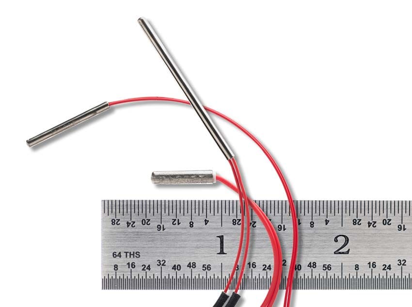
Burn-In Testing
Burn-in testing provides a statistical picture of the performance of a heater. The purpose of a burn-in test is to place a heater in typical controlled operating conditions and force it to fail. It is used to detect early failures using accelerated parameters and helps to ensure that a heater will perform as intended, up to expectations, and avoid possible problems for end users.
There are three potential failures that a heater may experience:
-
Early failure errors can be:
- Design flaws
- Specification misalignments
- Manufacturing errors
-
Use errors:
- Material malfunction
- Operational abnormalities
- Misuse
- Power surges
- Lifecycle exhaustion from wear and tear
Ovens used for burn-in testing can be simple, complex, or custom made with heating elements that provide reliable temperature control. The majority of ovens have stainless steel or tubular heaters that reach temperatures of 1200° F with a watt density of 40 watts per square inch.

Heaters for Semiconductor Manufacturing
Semiconductor production relies on thermal heating and precision control to ensure the quality, performance, and durability of semiconductors. Manufacturers choose heaters in accordance with the design of their process, with durability and resilience being the primary factors.
Polyimide Heater
A polyimide heater is made from Kapton, a polyimide film developed by DuPont. They have a very thin profile, are extremely flexible, offer excellent heat distribution, and have the necessary tensile strength. Polyimide heaters have an etched foil element of 0.0005 inches to 0.0001 inches thick compressed in two layers of polyimide film. They are excellent for extreme temperature conditions and maintain their shape regardless of temperature exposure.
Ceramic Heaters
Ceramic heaters have exceptionally fast heating and cooling, which makes them ideal for semiconductor production. They are made of thermally conductive aluminum nitrite ceramic with embedded tungsten resistance heating traces. Ceramic heaters are made in several unique configurations to serve as bonding instruments for semiconductor applications.
Tubular Heaters
Tubular heaters are highly versatile heaters that can be shaped and configured in any form and perform heat transfer by conduction, convection, or radiation. Since they can reach exceptionally high temperatures, they are ideal for industrial uses, such as the manufacture of semiconductors.
Brazed Heater Plates
Brazed heater plates have multiple minerals insulated heating elements for better uniformity and multi zone applications where single zone tubular heaters are unable to meet the necessary uniformity standards. They are made of stacked stainless steel plates that are brazed and corrugated to increase surface area and heat transfer.
Summary
Since thermal heating and temperature are such an important part of semiconductor manufacturing, there are heaters and heating elements capable of meeting the requirements of any semiconductor manufacturer. The wide choice of heating methods provides flexibility, precision, and exceptional control to the semiconductor production process.
Technology is Always Changing
The world of semiconductors is always changing. Whether it’s because of tensions between two countries, or new innovations trying to replace semiconductors all together, in 5-6 years the technology will likely be completely different.
The good news is, for now, you know enough to talk intelligently about semiconductors. So, go out there and impress people. Or at least make yourself look smart.
Resources
- https://electronics.howstuffworks.com/diode.htm
- https://www.wsj.com/articles/china-plans-47-billion-fund-to-boost-its-semiconductor-industry-1525434907
- https://spectrum.ieee.org/new-metalair-transistor-replaces-semiconductors
- https://techcrunch.com/2016/10/27/qualcomm-to-acquire-nxp-semiconductor-for-47-billion/
- https://theconversation.com/beyond-silicon-the-search-for-new-semiconductors-55795
- https://www.cnbc.com/2018/03/26/china-offers-to-buy-more-us-semiconductors-to-cut-trade-surplus-ft.html
- https://techcrunch.com/2018/05/07/china-chip-fund/
- https://www.ccn.com/blockchain-adoption-levels-highest-in-the-semiconductor-industry-accenture/
- https://newsroom.intel.com/news-releases/intel-supports-american-innovation-7-billion-investment-next-generation-semiconductor-factory-arizona/#gs.UAn82lU
- https://www.wsj.com/articles/u-s-startup-accuses-chinas-huawei-of-trying-to-steal-semiconductor-technology-1539867401
- https://techcrunch.com/2018/03/26/china-trades-semiconductors/
- https://bitcoinist.com/blockchain-iot-and-ai-push-global-semiconductor-sector-sales-to-over-40-billion/
- https://hardware.slashdot.org/story/18/12/01/188255/can-new-metal-air-transistors-replace-semiconductors-and-continue-moores-law
- https://www.investors.com/research/ibd-industry-themes/taiwan-semiconductor-apple-falls/
- https://www.used-line.com/semiconductor-and-pcb
- https://www.reuters.com/article/us-usa-trade-china-semiconductors-idUSKCN1N328E
- https://www.prnewswire.com/news-releases/global-semiconductor-sales-grow-as-the-industry-embraces-iot-and-blockchain-technology-881361928.html
 Castings & Forgings
 Bulk Material Handling
 Electrical & Electronic Components
 Flow Instrumentation
 Hardware
 Material Handling Equipment
 Metal Cutting Services
 Metal Forming Services
 Metal Suppliers
 Motion Control Products
 Plant & Facility Equipment
 Plant & Facility Supplies
 Plastic Molding Processes
 Pumps & Valves
 Recycling Equipment
 Rubber Products & Services